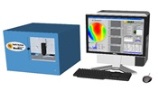
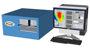
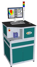
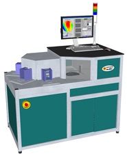
MaxMile EpiEL Mapping System
MaxMile EpiEL mapping system is a LED epi-wafer
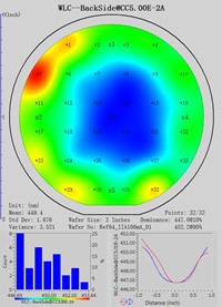
electroluminescence mapping system. It is a virtual LED device
fabrication & characterization system which can be used to measure
LED device parameters directly on epiwafers.
Without any costly and time-consuming device fabrication, EpiEL
reveals not only the electro-luminescence (EL) but also various
electrical properties of the material.
EL measurement is usually performed on finished
device (such as LED) since it needs a device structure to inject
current. MaxMile EpiEL technology overcomes this limitation by
instantly forming a well-defined LED device inside the material.
EpiEL test is nondestructive in nature. LED epi-wafer under test will
not be damaged and can be used as orignal wafer for next step use.
With such unique capability, MaxMile EpiEL technology provides an
unprecedented electroluminescence solution for optoelectronic
(especially solid-state lighting) industry which brings new
capability and better efficiencies:
-
Enabling
device-level quality control at early stage: MaxMile EpiEL
systems not only enable the device-level quality control right after
material growth, but also make it possible to perform such quality
control on every wafer (100% device-level quality control).
-
Providing instant response for LED material development: MaxMile
EpiEL systems can quickly obtain device-level information directly
on epiwafer right after material growth which provides nearly instant feedback for material
development such as recipe modification, growth & system
optimization, etc.
-
Enabling
"fabless" LED material and CVD system development: By
providing device-level characterization directly on epiwafer, MaxMile EpiEL systems enable
material or system development/improvement to be accomplished in a "fabless"
manner. In the past, any such development needs be verified through
costly and time-consuming device fabrication & evaluation.
-
Facilitating LED/LD research and development (R&D) with a powerful
tool: MaxMile EpiEL system is a virtual LED device
fabrication & characterization facility which
can be configured to simulate the different device structures. It can assemble quickly most device-level
optical and electrical properties of the material in a fabless manner
which could significantly reduce related R&D time and cost.
|